
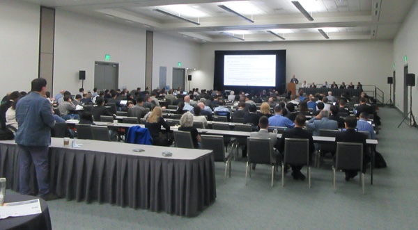
With an increasing momentum in photonic integration and last year’s OFC PIC Workshop attracting well over 350 attendees, this year will feature the seventh workshop on Photonic Integrated Circuits at OFC. The workshop is unique in the sense that it offers a material-independent one-stop-shop for anyone interested in or wanting to get started in photonic integration. The workshop is free of charge, but does require advance registration. Food and drinks will be provided and there is plenty of opportunity to network and interact with PIC service providers.
- The 7th Workshop on Photonic Integrated Circuits at OFC
- Wednesday March 11th, 2020 from 5:45pm to 8:30pm (with registration opening at 5:15pm)
- Room 29ABCD at the San Diego Convention Center
The advent of 100Gbps and beyond in both longhaul as well as datacom marked the breakthrough of photonic integration in a broader sense. As a result of this, PICs are now also being used e.g. in sensing, life sciences, and military applications and there is thus a growing group of people that are starting to design and use photonic chips.
However, the PIC value chain can be complex as one needs to make choices for the material system, the foundry and/or broker, the design and layout software, packaging solutions and so on. The aim of the PIC workshop is to bring together all the relevant players independent of material system and to provide an in-depth overview that allows you to make the right trade offs and to get to know the key PIC service providers. There will be a particular focus on multi-project wafer (MPW) shuttles together with the accompanying Process Design Kits (PDKs), since these substantially lower the cost of developing a PIC, provide a complete solution, create first-time right, and reduce the PIC development time.
The PIC workshop starts with a detailed overview of everything that you need to know in order to design, fab, and package a photonic chip. Subsequently there is a networking break during which you can interact with the key PIC service providers, who have table tops and provide useful information. During the break, food will be served and there will be drinks. After the break, there are several use case presentations by companies that are using photonic ICs and that are sharing their experiences.
OFC 2020 marks the 7th PIC workshop at OFC. Each year, we tried to improve the format and content of the workshop. Partly as a result, the OFC PIC Workshop attracted well over 350 attendees during the last few years. Starting in 2018, the group of supporting companies has widened by including more vendors of design and software solution as well as now also including providers of test & measurement equipment. This year, the use case section will focus on key trends and questions in photonic integration and there will be a dynamic panel discussion.
For any questions about the PIC workshop, please contact Erik Pennings at erik@7pennies.com or (848) 228-0807.
The PIC Workshop will be held on Wednesday March 11, 2020 from 5:15pm to 8:30pm, i.e. right after the conference and exhibition end for that day. The workshop takes place as part of the OFC conference and is held in Room 29ABCD of the San Diego Convention Center.

5:15 PM – 5:45 PM: Buffet Opens, Sponsor Tabletops and Networking
5:45 PM – 7:00 PM: Keynote Presentation “Latest Trends in Photonic Integration and How to Use the PIC Ecosystem to Develop a PIC Cheaper and Faster”
- Market Trends for Photonic Integration (Erik Pennings, 7 Pennies Consulting)
- InP-Based Integrated Photonics (Kevin Williams, JePPIX)
- Silicon Photonics (Bertrand Szelag, CEA LETI)
- Dielectrics/PLC Based Photonic Integration (Matt Curry, Broadex)
- Design, Simulation, and Layout Tools (Andre Richter, VPIphotonics)
- Packaging (Jeff Perkins, Avo Photonics)
- Test and Measurement (Pavel Zivny, Tektronix)
7:00 PM – 7:40 PM: Networking Break with Buffet and Sponsor Tabletops
7:40 PM – 8:10 PM: Use Cases and Key Topics in Photonics Integration
- Erman Timurdogan, Analog Photonics
- Gloria Hoefler, Infinera
- Michael Hochberg, Elenion
- Weiming Yao, Eindhoven University of Technology
8:10 PM – 8:30 PM: Panel discussion
- Question & answer on key PIC topics with panel consisting of all speakers and/or panelists from sponsoring companies
The workshop is supported by a wide group of service providers to the PIC industry. It includes foundries for pretty much all the relevant material systems, providers of simulation and layout software, packaging houses, test and measurement, as well as providers of turn-key PIC design solutions. The common denominator for most companies is that they support multi-project wafer (MPW) runs and process design kits (PDK), which are a great and cost-effective way to develop PICs.

Broadex Technologies specialises in the design and manufacture of integrated fibre optic components for the telecommunications and data communications markets. Founded in 2003 and headquartered in Jiaxing, China, Broadex Technologies has R&D and production facilities in Shanghai and Chengdu as well as Edinburgh, UK. Broadex specialises in the design and manufacture of long distance and PON transceivers, silicon photonics packaging and optical and opto-electronic packaging of splitters and WDM modules. Broadex Technologies’ Edinburgh site houses a world-class silica-on-silicon PLC design and manufacturing facility, which was established in 1998. It is the only 8” PLC fab in the world available to the market, which focusses on wafer-scale mass production of WDM and other telecommunications products. The Broadex engineering team have more than 20 years of experience in designing and optimising a wide range of PLC devices, including AWG-based multiplexers and demultiplexers, coherent mixer chips, rotator-combiner chips and interposers. For more information or to enquire about samples, please visit http://www.broadex-tech.com or email sales@broadex-tech.co.uk.

EXFO is a manufacturer of laboratory type fiber optic test instrumentation, not limited to, but primarily used in telecom type applications. Applications range from PIC design, research and development to manufacturing and production. EXFO’s product portfolio consists of high dynamic range tunable laser sources, automated wavelength dependent passive optical component testers, optical spectrum analyzers, tunable filters, and multipurpose modular test platform OSICS with modules ranging from tunable laser sources to switches, attenuators, DFB sources and more. (https://www.exfo.com)

Avo Photonics is the photonics industry’s trusted source for exclusive, private label photonics design, development, and manufacturing. We produce confidential, client-owned optoelectronic solutions and products for medical, military, industrial, aerospace and communications applications. Since 2003, we’ve earned the trust and confidence of these key markets for three important reasons:
- Optical, mechanical, thermal and electrical engineering are in our DNA. We were founded and are still guided by laser physicists and engineers who blend these critical, photonics-based disciplines into a single source for the conceptualizing, design, testing and producing of precision, rugged, optoelectronic components and assemblies.
- When we say confidential and client-owned, we really mean it. We work with market leaders that demand strict confidentiality and advanced technology that address their rapidly evolving photonics needs. When clients engage us, we become an extension of their organization. The knowledge and any patent-eligible intellectual assets we create become the sole property of our clients.
- Our AvoLight™ Services and our processes enable us to work with companies at nearly any stage of their product lifecycle. We become vested partners in their projects, delivering on-time and on-budget solutions regardless of their complexity, size or shape.
Avo is a U.S.-based company. Our Philadelphia, Pennsylvania facility houses our corporate headquarters, engineering, testing and manufacturing in a 41,000 square-foot building that features 22,000 square-feet of variable clean space for manufacturing. Design verification and prototyping are also supported at our Toronto, Ontario, facility. (http://avophotonics.com/)

VPIphotonics sets the industry standard for end-to-end photonic design automation comprising design, analysis and optimization of components, systems and networks. We provide professional simulation software supporting requirements of integrated photonics, optoelectronics and fiber optics applications, optical transmission system and network applications, as well as cost-optimized equipment configuration. Our team of experts delivers professional consulting services addressing customer-specific modeling and design requirements. VPIphotonics’ award-winning off-the-shelf and customized solutions are used extensively at hundreds of corporations worldwide; over 160 academic institutions joined our University Program. For further information, please visit us at www.VPIphotonics.com.

Luceda Photonics wants photonic IC engineers to enjoy the same first-time-right design experience as electronic IC designers. Luceda Photonics’ tools and services are rooted in over 50 years of experience in photonic integrated circuit (PIC) design. Photonic Integrated Circuit (PIC) design teams need full control of their design framework to make sure that what they fabricate matches exactly how they designed it. In addition they need to be able to re-use and distribute their design work in a hierarchical framework that saves time and improves reliability. IPKISS is a design platform that covers the complete photonic IC design flow up to measurement feedback for true component validation. What you layout is what you calculate. IPKISS.eda inside L-Edit combines these stringent photonic design demands with the ease of use of a professional yet easy to use EDA environment. (http://www.lucedaphotonics.com/en)

JePPIX is a broker that helps organizations around the globe to get access to advanced fabrication processes for Photonic Integrated Circuits (PICs). JePPIX aims at low-cost development of application specific PICs using a generic foundry model and rapid prototyping via industrial Multi-Project Wafer runs. The generic approach allows a variety of PICs to be realized using the same standardized processes. JePPIX closely collaborates with Europe’s key players in the field of photonic integration, including manufacturing and packaging partners, photonic CAD software partners, R&D labs and photonic IC design houses. With JePPIX you can get access to the Indium Phosphide (InP)-based monolithic integration platforms of Oclaro, Fraunhofer HHI and SMART Photonics and the low-loss dielectric TriPleX waveguide technology of LioniX. JePPIX is hosted by the Eindhoven University of Technology in the Netherlands. For more information visit our website: (www.jeppix.eu).

Photon Design was started in 1992 in Oxford UK to provide professional quality software to the photonics industry. Since that time it has introduced many innovations to photonics modelling, and now provides World-leading tools for the modelling of active and passive photonics components and circuits. Photon Design products are now in use in 30+ countries, 100s of research labs and contributed to 1000s of leading research publications, helping to develop the next generation of datacom components and innovations in micro and nano-optics. We are also able to provide custom solutions based on our standard products and our experts with decades of simulation experience are available for consulting. (https://www.photond.com)

FormFactor, Inc. (NASDAQ:FORM), is a leading provider of essential test and measurement technologies along the full IC life cycle – from characterization, modeling, reliability, and design de-bug, to qualification and production test. Semiconductor companies rely upon FormFactor’s products and services to accelerate profitability by optimizing device performance and advancing yield knowledge. The Company serves customers through its network of facilities in Asia, Europe, and North America. For more information, visit the Company’s website at www.formfactor.com.

As electronics become smaller and more capable, they become more complex. Necessary innovation must be met with ever-advancing technical capability. Tektronix designs and manufactures the test, measurement and monitoring solutions that break through the walls of complexity, to accelerate global innovation. Tektronix solutions have supported many of humankind’s greatest advances of the past 65 years. Health. Communication. Mobility. Space. We are committed to the scientists, engineers and technicians around the world who will define the future, and rely on us to embrace the technological challenge, as partners in their innovation (www.tek.com).

Chiral Photonics (CPI), a New Jersey, US based company founded in 1999, specializes in optoelectronic packaging of integrated photonics. CPI offers its pitch reducing optical fiber arrays, PROFAs, which enable the highest density optical I/Os for both edge and face coupling to photonic ICs. Currently, up to 61 I/O channels can be coupled in a single port. Other services range from single-die optical coupling or optoelectronic package development, including test services, to volume optoelectronic production packaging.Please contact us to obtain our free coupling and packaging design guidelines: designguide@chiralphotonics.com.

Innovations for the digital society of the future are the focus of research and development work at the Fraunhofer Heinrich Hertz Institute HHI. In this area, Fraunhofer HHI is a world leader in the development of mobile and optical communication networks and systems, fiber optical sensor systems as well as the processing and coding of video signals. Together with international partners from research and industry, Fraunhofer HHI works in the whole spectrum of digital infrastructure – from fundamental research to the development of prototypes and solutions. The institute develops standards for information and communication technologies and creates new applications as an industry partner. (www.hhi.fraunhofer.de)

CEA (Commissariat à l’Energie Atomique et aux Energies Alternatives) is a French Governmental Research Organization (15,000 employees). Within the “CEA-TECH” branch devoted to industrial Research & Development, CEA-LETI is one of the major European research centers in applied electronics, optics and sensing. It is located in Grenoble-France where it operates 11,000 m²-State-of-the-Art CMOS clean rooms (200 and 300 mm wafer size), and a MEMS microsystems platform (200 mm wafer size). Nearly 1,600 men and women are serving innovation and the transfer of technology in key domains. Besides, CEA-LETI has sparked the creation of thirty high-technology start-ups, including Soitec, world leader in the development/ production of Silicon on insulator wafers.
As a pioneer in Research & Development in Silicon Photonics (since 2002), CEA-LETI has developed strong expertise and know how in the design, fabrication and test of integrated devices (including Ge-on-Silicon photodetectors and hybrid III/V-on-Silicon lasers) and circuits for telecom and datacom applications. ST microelectronics is one of its main industrial partner in the field. (http://www.cea.fr/english/Pages/cea/the-cea-a-key-player-in-technological-research.aspx)

Keysight Technologies Inc. is the world’s leading electronic measurement company, transforming today’s measurement experience through innovations in wireless, modular, and software solutions. With its HP and Agilent legacy, Keysight delivers solutions in wireless communications, aerospace and defense and semiconductor markets with world-class platforms, software and consistent measurement science. The company’s nearly 10,500 employees serve customers in more than 100 countries. (Keysight Technologies)

Lumerical develops photonic simulation software – tools which enable product designers to understand light, and predict how it behaves within complex structures, circuits, and systems. Since being founded in 2003, Lumerical has grown to license its design tools in over 50 countries and its customers include 13 of the top 15 technology companies in the FORTUNE Global 500 index, and 47 of the top 50 research universities as rated by the Times Higher Education rankings. Lumerical’s substantial impact on the photonic design and simulation community means its tools are among the most widely cited in the scientific press, with references in more than 14,000 scientific publications and patents. Lumerical enables its customers to achieve more with light and establish a leading position in the development of transformative technologies employing photonics. (www.lumerical.com)

OSA Industry Development Associates (OIDA) Membership–Delivering Business Value through Best-In-Class Member Benefits and Exceptional Advocacy. OIDA membership provides an immediate return on investment through: powerful advocacy to policymakers and other stakeholders, business and networking opportunities, Industry intelligence and benchmarking and discounts on promotional opportunities and events. (http://www.osa.org)
Please find below here the bios, pictures and logos for the key note speakers, the use case speakers, as well as the panel participants. Please note that we’re in the process of confirming additional speakers and will update the list shortly.

Dr. Gloria E. Höfler holds Ph.D. M.S. and B.S. degrees in Electrical Engineering from the University of Illinois at Urbana-Champaign. Her career has spanned development of optoelectronic materials and devices ranging from R&D stage, new product innovation to high-volume manufacturing at 3M’s Corporate Research Laboratories, HP’s Optoelectronic Division, LumiLeds Lighting, Agilent Technologies, Corning and Infinera. She has co-authored over 70 peer-reviewed and invited papers and holds multiple patents in the area of optoelectronic devices. She is an SPIE Fellow and an IEEE Sr. member. Currently, she is Director of Advanced Development at Infinera, leading the InP Photonic Integrated Circuits (PICs) Foundry offering and EPDA development.

Michael Hochberg’s career has spanned the space between fundamental research and commercialization since his time as an undergraduate in physics at Caltech. He and his collaborator, Tom Baehr-Jones, developed a design tool for the accurate simulation of silicon photonic components as part of their research and spun the effort off as a company called Simulant. He co-founded his second company in silicon photonics, Luxtera, during his senior year. After returning to Caltech for his post-graduate degrees, he completed his MS and Ph.D. in applied physics at Caltech in a total of three years. Since that time, Michael has held faculty positions and run research groups at the University of Washington, University of Delaware, and the National University of Singapore, and has held appointments in various departments including Electrical Engineering, Chemical and Biomedical Engineering, and Materials Science. He currently holds a visiting appointment at Columbia University. Michael was the Director of the OpSIS foundry-access service, which built a community of hundreds of silicon photonic designers around the world. OpSIS was the first organization to offer silicon photonic multi-project wafer runs including a library of passive devices, high-speed modulators and detectors, and an integrated PDK. Michael has won a number of awards for his work, including an NSF Graduate Research Fellowship, the Demetriades-Tsafka Prize for the best thesis by a graduating Ph.D. student in the field of nanotechnology at Caltech, a U.S. Air Force Young Investigator Program Award, a Singapore National Research Foundation Fellowship, and a Presidential Early Career Award in Science and Engineering, which is the highest honor granted by the US government to young scientists. He has published numerous papers and patents, and his work has been cited over 10000 times in the scientific literature.

Dr. Erman Timurdogan is the Director of PDK development and Optical Communications at Analog Photonics (AP). He is leading a team to develop the Process Design Kit (PDK) component library and Silicon Photonics (SiPh) optical transceiver product line. With his contribution, AP_SUNY PDK includes 60+ verified passive and active SiPh components for O and C+L bands for various photonic applications. He also serves as the chief architect and team lead for 400G and +1T co-packaged optics and on-board optics SiPh transceiver development. He has gained technical and program management skills in writing SBIRs, government contracts, industrial proposals and on-time execution of milestones and critical deliverables. Dr. Timurdogan received his Ph.D. and M.S. in electrical engineering and computer science from Massachusetts Institute of Technology (MIT) and B.S. in electrical and electronics engineering from Koc University (KU). At MIT, he designed, developed and demonstrated the operation of highly reliable ultra-low-power 3D integrated electronic-photonic silicon transceivers on 300mm silicon-on-insulator wafers. He has authored 75 peer-reviewed publications, 12 patents and book chapters which were cited over 1800 times.

Weiming Yao is an Assistant Professor in the Photonic Integration research group of Professor Kevin Williams at Eindhoven University of Technology (TU/e). His key field of expertise is in high-speed optical components, semiconductor lasers and high-density photonic integrated circuits (PICs). Currently, he is working on ways to intimately connect photonic circuits with electronics and further improve on speed and density of PICs. A new field of interest is neuromorphic photonics, where he explores the possibilities of building neural networks in photonic circuits.

Nathan Soper has spent the last two years managing technical sales at Photon Design across Europe and the USA. He began working in integrated photonics as an undergraduate working on athermal ring resonators. This lead into a PhD in Silicon Photonics at the University of Southampton, specialising his research in simulation and fabrication methods for high-volume packaging applications.

Dan Neugroschl received the M.S. degree in materials science from Columbia University, New York, NY, USA. He is currently the President of Chiral Photonics, Pine Brook, NJ, USA, which he cofounded in 1999.

Pavel Zivny is a high speed serial data Domain Expert with the wide band oscilloscopes group of Tektronix. Pavel has a number of oscilloscope related patents, papers and articles, and represents Tektronix and T&M on industry panels and program committees, e.g. IEEE 802.3cd Ethernet. His current interests in the high speed serial data field include Equivalent Time Sampling and Real-Time oscilloscope measurements as well as signal generation with BERTs and Pattern Generators.

Dr. James Pond is the CTO and co-founder of Lumerical Inc. and is a driving force behind the company’s core software algorithms, technology, and advanced photonic modeling capabilities. He has almost two decades of experience in optical and photonic simulation, and is the author of numerous papers, patents and conference presentations.

Matthew Currie is the Head of Sales and Marketing at Broadex Technologies, responsible for global sales and marketing activities outside of China. Matthew completed an MSc in Nanotechnology and Microsystems followed by an EngD in Photonics at Heriot-Watt University. Prior to joining Broadex Technologies he was the Applications Engineering Manager for PowerPhotonic where he was instrumental in developing the micro-optical product catalogue and core laser micromachining technology, authoring several patents on optical designs and manufacturing before transitioning to a technical customer facing role. With his strong engineering background, Matthew has a keen understanding of his customers’ needs within a high-technology product landscape. He is now focussed on taking a proactive and customer-centred approach to design, develop and manufacture innovative new PLC products for the telecommunications market.

François Couny is Product Line Manager for EXFO Optics. He started his career in 2001 as a Test & Measurement engineer at Blaze Photonics, a start-up company specialized in Photonic Crystal Fibre and completed his Ph.D. in Photonics in 2008 at the Centre for Photonics and Photonic Material at the University of Bath (UK). He went on to join Yenista Optics in 2010 with a focus on developing tuneable laser sources and spectral solutions, including an Optical Spectrum Analyzer and also an optical component tester adapted to photonic integrated circuits characterization. Since 2015, François has been PLM for Yenista Optics, now part of EXFO as EXFO Optics.

Pieter Dumon is CTO of Luceda Photonics. He obtained the EE MSc and PhD degrees from Ghent University in 2002 and 2007, respectively, with a dissertation on silicon photonics wavelength filter devices. Peter contributed to the imdc silicon photonics platform and coordinated ePIXfab, the first multi project wafer service for photonics ICs, from 2007 to 2014. He grew ePIXfab to a network of partners, offering chips, packaging and design services to world-wide industry and academic customers. Being fascinated by software, semiconductor technology and manipulating light on tiny chips, Pieter co-founded Luceda in 2014.
Kevin Williams is a Full Professor and Chair of the Photonic Integration research group at Eindhoven University of Technology (TU/e). His key fields of expertise include photonic integrated circuits, semiconductor lasers and their application in communications and sensing. Kevin’s research group explores the scaling properties of photonic circuits, enabling faster and more energy-efficient components and circuits. The group builds on its know-how in active-passive monolithic InP integration, creating circuits with lasers, amplifiers, energy-efficient quantum well modulators, detectors, power splitters, filters and more all on the same chip. This is addressed within three main themes: Generic integration – a methodology for enabling many different circuits using the same platform technology and an important vehicle for researching and validating the latest photonic devices and processes. Heterogeneous and hybrid integration – the technologies for combining and co-designing photonic components and circuits with Silicon Electronics and dielectric materials, Integrated nano-photonics – using InP membranes on Silicon for the miniaturization of components and the leveraging of sub-wavelength photonic structures in circuits. Kevin teaches courses in design, electronics and photonics.

André Richter is an expert with 20+ years of experience in the field of optical communications and photonics. He received his M.Sc. degree from Georgia Tech, USA and Ph.D. from TU Berlin, Germany. André co-authored 100+ publications and contributed to 15+ international R&D projects. Being with the VPIphotonics team since 1997, André generated numerous novelties in industry research and education, commercialization and market development. He held management positions with responsibilities for technical services, product management, research & development before being appointed as General Manager in 2013.

Dan Rishavy is a Director of Market Development for FormFactor’s systems business unit. Dan holds a degree in Electrical Engineering from the University of South Florida and an MBA from West Texas A&M University. He has been working in various aspects of the Semiconductor Test and wafer probing industry for over 20 years. Dan has held variety of roles in applications, product management and marketing throughout his career at Hewlett Packard, Agilent, Verigy, Tokyo Electron, Cascade Microtech, and Form Factor.

Hansjoerg Haisch is program manager for networks & data center solutions within Keysight Technologies’ communication solutions group. He has been responsible for definition and development of test and measurement products and solutions for photonic component and transmission test, lately for digital coherent transmission and integrated and Silicon photonics. Hansjoerg joined Agilent Technologies in 2001 as R&D project manager. Hansjoerg started his career as R&D engineer for opto-electronic components in the Alcatel Research Center Germany in 1990, responsible for the design and characterization of opto-electronic components. Later he managed projects for high speed transmission, CaTV and fixed wireless networks in Alcatel research and product divisions. Hansjoerg holds a Ph.D. from Stuttgart University and a Master of Science from Oregon State University both in Electrical Engineering.

Jeffrey Perkins, PhD, is the COO for Avo Photonics. With broad experience in high-volume optical component production, he joined Avo Photonics from JDSU where he served as Director of Manufacturing Engineering, Technical Manager of Process Development and Automation, and Senior Technical Manager of Product Development. Prior starting in the optoelectronics industry in 1999, Dr. Perkins held technical positions in microelectronics packaging for IBM in Endicott, New York. Jeff holds a PhD in Mechanical Engineering from Lehigh University in Bethlehem, Pennsylvania.

Dr Bertrand Szelag received the Master degree in Physics from the University of Lille in 1994 and the PhD degree in Microelectronics from the University of Grenoble in 1999. He has been a visiting researcher in Tohoku University in 1997 working in the field of sub-100nm CMOS transistor properties. In 1999 he joint STMicroelectronics in Crolles, France to work on BiCMOS platfrom development for Analog/RF applications. Since 2013, he has been with the LETI, MINATEC Institute, Grenoble, France as a Project Manager and senior process integration researcher in the field of silicon photonic devices. His current research activities included high speed silicon modulator, germanium photodetectors and hybrid III-V laser integration in silicon. He is the author or co-author of more than 50 papers in scientific journals and international conference proceedings in the field of CMOS, Bipolar and DMOS transistors and silicon photonic devices.
PIC ARCHIVE
For more info, please check out the archived earlier photonic integration events. Material for these events has been posted and is available on request.